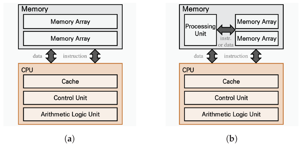
As data-intensive applications continue to dominate modern computing, traditional architectures face growing challenges in handling the massive flow of information between processors and memory. This has led to one of the most transformative developments in semiconductor engineering: Processing-in-Memory (PIM).
By integrating computation directly within the memory components, PIM significantly reduces data movement, power consumption, and latency, offering a paradigm shift for VLSI circuit design and modern chip designing practices.
Understanding Processing-in-Memory (PIM)
Processing-in-Memory refers to an architectural approach that allows data processing to occur directly within memory arrays, rather than sending data back and forth between separate memory and processor units.
Traditional architectures, often referred to as the von Neumann model, suffer from what’s known as the “memory wall”; a bottleneck that arises when the processor waits for data to move from memory. PIM removes this inefficiency by embedding logic operations within the memory itself.
This concept enables higher computational efficiency for data-heavy tasks like artificial intelligence, machine learning, image recognition, and database acceleration.
Why Data-Centric Architectures Need PIM
As workloads evolve to process unstructured, high-volume data streams, the need for data-centric VLSI architectures becomes increasingly evident. The rapid growth of big data analytics and cloud computing requires systems that can manage and analyze massive data sets locally, without overburdening memory bandwidth.
PIM plays a vital role here by:
- Reducing Data Transfer Overhead: Computation within memory minimizes traffic between processor and memory.
- Lowering Energy Consumption: Since data movement accounts for nearly 60% of system power in conventional designs, PIM offers substantial energy savings
- Boosting Parallelism: Integrated memory computation allows for parallel data processing across memory arrays.
The combination of performance gains and power efficiency makes PIM a cornerstone of future VLSI circuit and system design innovations.
PIM’s Impact on Chip Designing
From a chip designing perspective, PIM introduces both new opportunities and design complexities. Engineers must integrate computational logic within the memory hierarchy, requiring novel approaches to transistor-level design, logic optimization, and memory interfacing.
Traditional design tools are evolving to accommodate hybrid memory-compute layouts. Simulation frameworks now consider how on-memory processing units impact thermal distribution, signal integrity, and circuit timing.
Moreover, new materials and memory technologies, such as MRAM and ReRAM, are emerging as ideal candidates for PIM implementation due to their non-volatility and scalability.
Architectural Innovations Enabled by PIM
Several architectural advancements are being realized through PIM integration:
- In-Memory AI Accelerators: Specialized PIM chips enhance deep learning inference by reducing memory access latency.
- Heterogeneous Computing Systems: PIM modules complement CPUs and GPUs by handling parallel, memory-intensive workloads.
- Edge Computing Efficiency: Localized computation within sensors and embedded devices lowers dependence on cloud-based processing.
By embedding logic near data, designers can achieve superior performance for workloads that rely heavily on data movement.
The Role of PCB Design in PIM-Enabled Systems
The evolution of PIM also influences PCB design board layouts. As PIM-based chips introduce new interconnect and thermal considerations, printed circuit boards must be optimized for power delivery, signal timing, and heat management.
PCB engineers play a critical role in maintaining signal integrity across densely packed data paths. Careful trace routing, grounding, and impedance matching ensure that high-speed data transfers remain stable even as computation moves closer to memory.
Innovative PCB stacking and 3D integration techniques are becoming essential to accommodate the rising demand for compact, efficient PIM-based systems.
Design Tools and Testing for PIM-Based VLSI Circuits
As PIM technology matures, VLSI circuit verification and testing processes are also evolving. Since logic and memory are combined, traditional fault models need to be adapted to detect errors in both computation and storage operations. Built-in self-test (BIST) mechanisms and adaptive diagnostic algorithms are being developed to ensure reliability under complex workloads.
Additionally, electronic design automation (EDA) tools are being upgraded to simulate the concurrent activities of compute and memory units. Accurate thermal, power, and timing analysis tools help designers predict how PIM-enabled architectures will perform under real-world conditions.
In large-scale deployments, machine learning algorithms are even being used to optimize design parameters automatically, reducing the time and cost of silicon validation.
Challenges in Implementing PIM
While PIM offers enormous potential, it also presents design challenges that the semiconductor industry must overcome. These include:
- Integration Complexity: Balancing memory density with compute functionality.
- Thermal Management: Increased computation within memory leads to localized heating.
- Programming Models: Traditional software models need to evolve to leverage in-memory computation effectively.
- Testing and Verification: Ensuring functional reliability in hybrid memory-compute architectures remains a major focus area.
Ongoing research and collaboration between academia and industry continue to refine these challenges, paving the way for PIM to become a mainstream design choice.
Future Outlook: PIM and the Next Generation of VLSI Design
PIM will redefine how VLSI circuits are conceptualized and designed in the coming decade. Its integration into next-generation architectures will enable more efficient machine learning accelerators, intelligent edge devices, and high-performance computing systems.
As fabrication technologies shrink and data demands grow, PIM’s energy efficiency and computational density will be key factors in achieving scalable, sustainable performance.
The industry’s focus is gradually shifting from pure processing power to data movement efficiency, and PIM sits at the heart of this evolution.
Conclusion
The rise of Processing-in-Memory marks a fundamental change in how chips are designed and optimized for data-driven workloads. By merging computation and storage, PIM eliminates long-standing bottlenecks, setting a new standard for VLSI circuit innovation and chip designing excellence.
As PIM continues to mature, companies equipped with advanced design, testing, and PCB design board expertise will lead the way in creating faster, more efficient, and intelligent systems.
Tessolve is a global leader in this transformation. With two decades of semiconductor engineering excellence, over 3500 professionals across 12 countries, and partnerships with leading chipmakers, Tessolve empowers semiconductor companies with end-to-end solutions from IC design and PCB development to test, validation, and product engineering.
Contact Tessolve today to learn how our expertise in silicon, systems, and semiconductor engineering can help accelerate your innovation in the PIM-driven era of VLSI design.


